

Never Miss a Beat: Get a snapshot of the issues affecting the IT industry straight to your inbox.
IBM Nanotube Researcher Explains Breakthrough
IBM lead researcher Shu-Jen Han explains the significance of finding an effective connector for 7-nanometer nanotube transistors.
4 Min Read
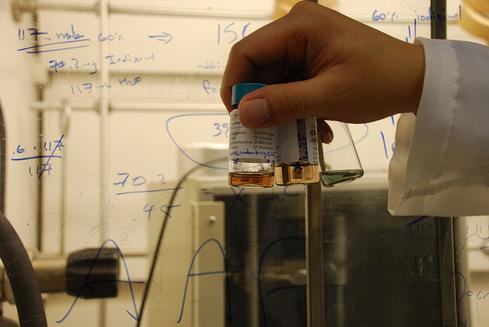
<p align="left">Carbon nanotubes in solution</p>

Apple, Microsoft, IBM: 7 Big Analytics Buys You Need to Know
Apple, Microsoft, IBM: 7 Big Analytics Buys You Need to Know (Click image for larger view and slideshow.)
Why is the discovery of a method for fusing metal connectors to carbon nanotube transistors a big deal? Shu-Jen Han, manager of the Nanoscale Science and Technology Group at IBM in Yorktown Heights, N.Y., explains why.
CPUs based on nanotubes are expected to lead to denser computing architectures, both in the cloud and the enterprise data center. And those gains will be matched by more powerful smartphones and handheld computers with much longer battery lives.
However, as Han explained, as transistors shrink, their connectors shrink as well.
Wouldn't those two things be a compatible set of developments?
Actually, no, Han said in an interview with InformationWeek. As the connector shrinks, its resistance rises until -- at very small sizes, say 10 nanometers -- it acts as a drag on the performance of the CPU as a whole. The electrons, or electron holes as the case may be, traversing the transistor struggle to get through the gate represented by the connector.
By the time it's shrunk to 10 nanometers, it is so small that "it doesn't have enough room for electrons to flow into the channel (the nanotube transistor)," or vice versa, out of the channel, said Han.
Han drew an analogy between carbon nanotubes and their connectors and a freeway with its exits. It doesn't matter how high a speed you can achieve on the freeway if the exit is so small that you have to slow down to get through it. The too-small exit ramp has been the case so far with carbon nanotubes, he said.
That was the problem confronted by IBM nanotechnology researchers as they attempted to build a nanotube transistor. The carbon nanotube is an excellent semiconductor and actually moves the charge (or the absence of it, in the case of an electron hole) 10 times faster than silicon semiconductors. Since nanotubes can be made that are smaller than today's smallest circuits, they appear to be an ideal material with which to build transistors into the sub-10 nanometer range.
However, unless the connector can continue to shrink in step with the transistor, the prospect of smaller, denser CPUs and more powerful compute engines remains a pipedream. Nanotubes functioning in isolation in the lab as a proof of concept were basically useless without high function connectors.
Han's research team has found molybdenum to be the metal best suited for nanotube connectors.
"We've tried many different metals. Molybdenum gives us the best performance," Han said. Instead of a physical process, such as soldering or etching, the connection between the nanotube and molybdenum contact is formed by a metallurgical process -- a chemical bond that fuses the metal to the tip of the nanotube.
[Want to learn more about IBM carbon nanotubes? See IBM Nanotube Breakthrough Will Create Low Power, Faster CPUs.]
"Our novel approach is to make the contact from the end of the carbon nanotube, which we show does not degrade device performance. This brings us a step closer to the goal of a carbon nanotube technology within the decade," said Han.
In addition to good semiconductor properties, nanotubes have good heat dissipation or thermal conduction properties, which is another reason it's thought they can be assembled in very high concentrations for CPUs. Transistor for transistor, they generate less heat than silicon chips to begin with because they require less power.
All nanotube researchers tend to hedge on the timeframe in which their breakthroughs will become products. Han said IBM is capable of building 7 nanometer transistors out of nanotubes today but would be more likely to put a smaller transistor into component production, say 3-5 nanometers. If it pushed ahead at 7 nanometers, the industry could expect nanotube CPUs in five years, he said. If it invests in a smaller size, then it will be five to 10 years before such components emerge.
Intel is already producing 14-nanometer Broadwell and Skylake chips but has announced delays in its planned move to 10 nanometers. The fact that silicon semiconductors are slated to move to that diminutive circuit size will probably push IBM to a more distinctively small dimension than 7 nanometers.
Unlike silicon chips, researchers are still working on a good substrate on which to mass-produce nanotubes.
"We don't have a carbon nanotube wafer," Han said. But he doesn't think the substrate is nearly as big an issue as the connectors. Nanotubes will self-assemble either in-line or side-by-side as they're produced in ways that can be manipulated as researchers learn more about them, he predicted.
About the Author(s)
You May Also Like
More Insights
Webinars
How to Amplify DevOps with DevSecOps
May 22, 2024Generative AI: Use Cases and Risks in 2024
May 29, 2024Smart Service Management
June 4, 2024
Editor's Choice


May 2, 2024
While there are plentiful options in cyber resiliency and business continuity tools and platforms, there isn’t one that can knock out everything from sudden cloud outages to prolonged ransomware attacks in a single punch. What can you do to keep the company on its feet no matter what is thrown at it? Find out in this new virtual event.
Reserve Your Seat Now